Marcelo Antunez
Senior PCB Design Engineer · Lawyer (OAB/SP, Brazil)
PCB Design Engineer with 25 years of experience in high-reliability printed circuit boards: first in defense and aerospace systems (IPC Classes 2 and 3, HDI) and, since 2026, in DDR4/DDR5 DRAM memory modules in the semiconductor industry.
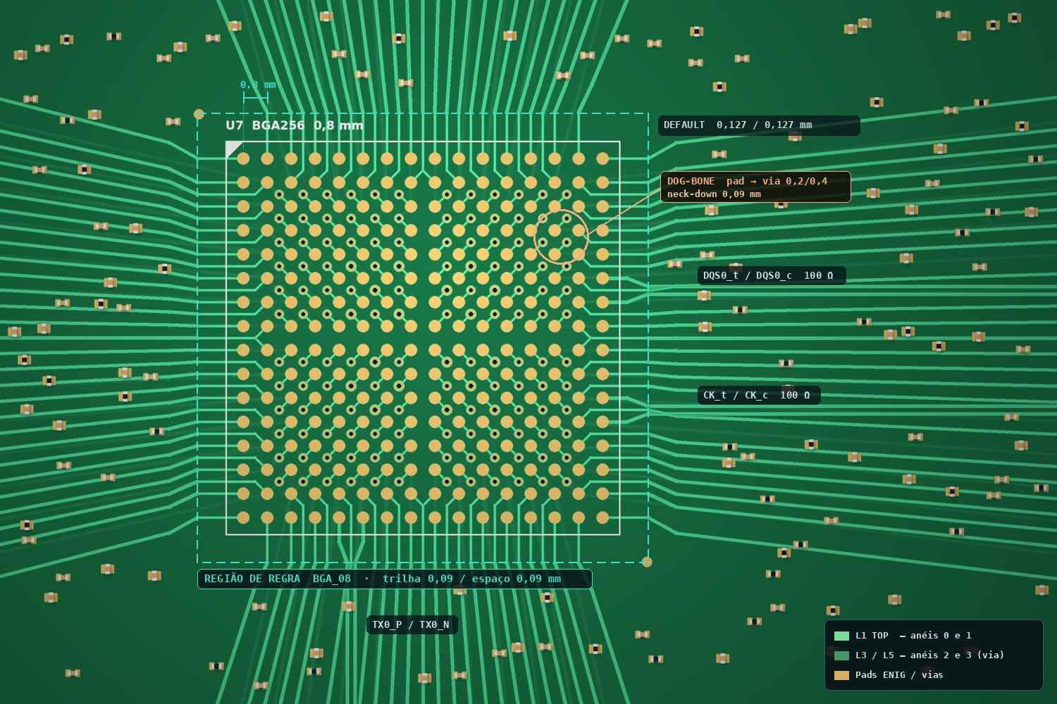
Works from schematic to fabrication release, with signal-integrity-driven layout: stackup, impedance control, differential pairs and length/delay matching.
Areas of expertise
Multilayer and HDI
Layouts up to 12 layers and HDI Types I, II and III: placement, routing, stackup and impedance.
High speed / SI
Differential pairs, length/delay matching and signal-integrity constraints.
DDR4/DDR5 memory
SO-DIMM, UDIMM and RDIMM modules and test boards, per JEDEC standards.
Aerospace RF
Wraparound antenna boards for aerospace applications.
Libraries and schematics
Corporate libraries (IPC-7351), Capture CIS database, templates and DRC rules.
Manufacturing and ESD
Gerber/ODB++ documentation, DFM/DFA, fabricator interface and ANSI/ESD S20.20 program.
Cadence Allegro X PCB Editor (Basic, Intermediate and Advanced, 2026) · OrCAD Capture / Capture CIS
IPC-2221 · IPC-7351 · IPC-A-610 · ANSI/ESD S20.20 · JEDEC
Electrical and Electronics Engineering (ETEP) · Electronics Technician · Law (OAB/SP)
International experience: April to June 2026 in Shanghai (China), on memory test boards focused on impedance, signal integrity and rigid-flex.
Engineering + Law: legal training supports the interface with suppliers on contracts, intellectual property and compliance.